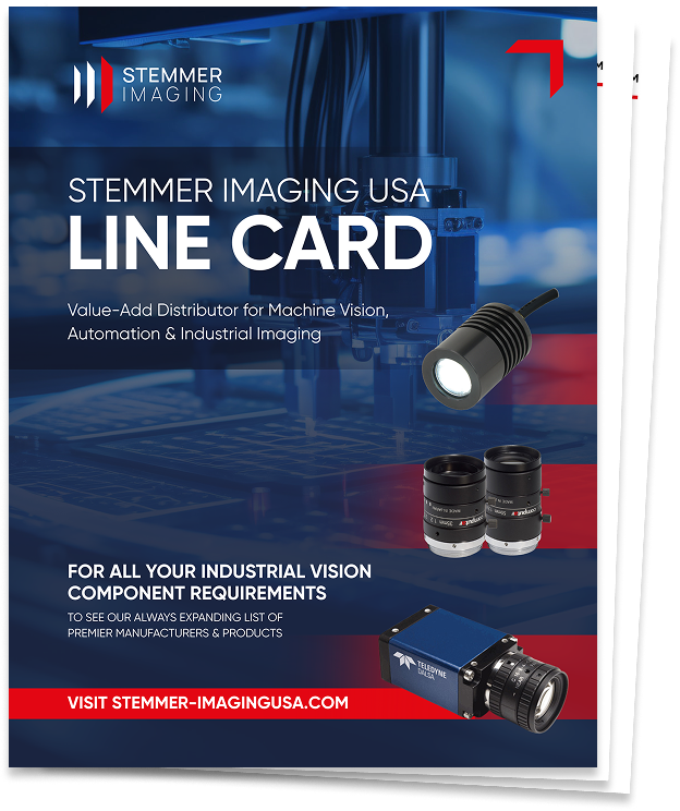
40+ Premier Vision Manufacturers
Download our comprehensive line card to browse premier brands across cameras, lenses, lighting, and sensors.

Precision Vision Components for Semiconductor Manufacturing
Advances in semiconductor manufacturing technology are driving the development of higher performance vision systems. With higher vision processing speeds and resolutions, as well as greater hardware and software requirements, new standards such as Camera Link HS, and CoaXPress are being developed. OEM's are taking advantage of these new standards to develop next generation inspection equipment for high-volume wafer production, testing, and packaging. The goal is to reduce inspection time and improve quality, while adapting easily to different wafer sizes.
Capturing defects at each point of the manufacturing process is critical in semiconductor manufacturing. Cameras, frame grabbers, lighting and software all play an important role in the various inspection processes that are conducted during the different steps required to turn silicon into working chips. This environment creates an industry demand for more powerful, higher resolution, higher speed, low light cameras. OEMs in this market are the real technology drivers of the future, and therefore are always seeking state of the art solutions, in order to ensure profitable business results.
Your Trusted Partner Since 1986
STEMMER IMAGING USA has been assisting OEMs, system integrators, and end-users with vision components since the dawn of the vision industry. A premiere, vertically-integrated distributor since 1986, STEMMER IMAGING USA offers you access to an extensive inventory of the industry's premier manufacturers of CCD and CMOS cameras, cables, image acquisition boards, lenses and software products. Our application specialists provide industry insight and guidance to help you select the right products to achieve your specific results.
LEARN MORE ABOUT OUR HISTORYKey Vision Applications in Semiconductor Equipment
Wafer Surface Inspection
Ultra-high-resolution cameras with specialized optics detect microscopic defects, scratches, particles, and contamination on silicon wafer surfaces. Line scan and area scan cameras operating at high speeds inspect entire wafer surfaces, identifying defects measured in nanometers that could compromise chip functionality or yield.
Pattern Defect Detection
Advanced imaging systems verify that photolithography patterns are correctly formed on wafers, detecting missing features, bridging, and dimensional variations. High-resolution sensors and precise optics enable detection of pattern defects at the sub-micron level, ensuring circuit integrity across the entire wafer.
Die Inspection & Sorting
Vision systems inspect individual die for defects, verify proper singulation, and guide pick-and-place equipment for die sorting and packaging. High-speed cameras enable 100% inspection at production rates, maximizing yield by identifying and removing defective die before packaging.
Package & Bond Wire Inspection
Cameras with specialized lighting and high magnification lenses inspect wire bonds, ball bonds, and package integrity. Vision systems detect wire sweep, insufficient bonds, missing wires, and package cracks that could cause device failure, ensuring reliability in finished semiconductor products.
Alignment & Registration
Precision vision systems provide accurate alignment and registration for lithography, bonding, and assembly processes. Sub-micron positioning accuracy ensures proper layer-to-layer alignment and component placement critical to semiconductor device functionality and performance.
Metrology & Dimensional Measurement
High-precision measurement systems verify critical dimensions of features, layers, and structures throughout the manufacturing process. Telecentric optics and high-resolution sensors enable accurate measurement of feature sizes, layer thickness, and dimensional tolerances essential for process control.
Don't see your specific application? Contact STEMMER IMAGING USA to discuss your custom needs.
Advanced Vision Technologies for Semiconductor Applications
Semiconductor manufacturing demands the highest performance imaging components available, operating at speeds and resolutions that push the boundaries of vision technology. Key Technologies Available:
- Ultra-High-Resolution Cameras with multi-megapixel sensors for wafer inspection
- High-Speed Camera Link and CoaXPress Interfaces for extreme data throughput requirements
- Line Scan Cameras optimized for continuous wafer and substrate inspection
- Specialized Semiconductor Optics including telecentric and microscopy lenses
- Advanced Lighting Solutions for enhanced contrast and defect visibility
- Frame Grabbers with High Bandwidth supporting multiple camera configurations
- Low-Light and High-Sensitivity Sensors for challenging inspection tasks
- Machine Vision Software with advanced defect detection algorithms
These components from leading manufacturers enable OEMs to build next-generation semiconductor inspection equipment that meets the demanding requirements of modern chip fabrication.
BROWSE OUR TRUSTED BRANDSBenefits of Semiconductor Vision Systems
Maximum Yield & Defect Reduction
High-resolution vision systems detect microscopic defects early in the manufacturing process, preventing defective wafers from consuming expensive processing steps. Early detection maximizes yield by identifying and removing problematic wafers, die, or devices before additional value is added, directly impacting profitability.
Extreme Precision & Accuracy
Vision components provide measurement and inspection accuracy at the nanometer scale, essential for current and next-generation semiconductor devices. Sub-micron positioning and defect detection capabilities ensure that even the smallest anomalies are identified, maintaining the quality standards required for advanced chip production.
High-Speed Throughput
Advanced camera interfaces and high-speed imaging sensors enable inspection at the rates demanded by high-volume semiconductor manufacturing. Vision systems process massive amounts of image data in real-time, keeping pace with production equipment while maintaining inspection quality and accuracy.
Process Control & Continuous Improvement
Comprehensive inspection data provides valuable feedback for process optimization and yield enhancement initiatives. Vision systems identify trends and correlations between process parameters and defect rates, enabling continuous improvement in manufacturing processes and equipment performance.
Need Help Selecting Semiconductor Vision Components?
Tell us about your semiconductor inspection application and our specialists will recommend the ideal products from our extensive manufacturer portfolio.